What's all this about Watts, Volts, and Amps? Good question.
Here's the extremely short answer. Conductive objects are always full of movable electric charges, and electric currents are motions of these charges. Voltage pushes the conductors own charges along. A conductor has a certain amount of electrical resistance or "friction," and friction with the flowing charges heats up the resistive object. The flow rate of the moving charges is measured in Amperes, while the transfer of electrical energy (as well as the rate of heat output) is measured in Watts. The electrical resistance is measured in Ohms. Amperes, Volts, Watts, and Ohms. Simple? Let's take a much deeper look.
First the watts and amperes. Watts and amps are somewhat confusing because both are flow rates, yet we rarely talk about the STUFF that is flowing. It's difficult (if not impossible) to understand a flow rate without understanding the flowing substance. Think about it: could we ever understand water-flow without first grasping the "water" concept?!
Electric current isn't a stuff. Electric current is the flow of a stuff. What's the name of the stuff that flows during an electric current? The flowing stuff is called "Charge."
AMPERES
What flows in wires? It has several names:
• Charges of electricity
• Electrons
• Electric charge
• Electrical substance
• Electron-fluid
• "Charge-stuff"
A quantity of charge is measured in units called COULOMBS, and the word "ampere" means the same thing as "one coulomb of charge flowing per second." If we were talking about water, then Coulombs would be like gallons, and amperage would be like gallons-per-second.
Why do I say that amperes are confusing? Simple: textbooks almost always teach us about amperes and current without first clearly explaining the coulombs and charge! Suppose that you had no name for "water," yet your teachers wanted you to learn all about "flow" inside metal pipes? Suppose you had to understand "gallons-per-second," but you had to do this without knowing anything about water or about gallons.
If you'd never learned the word "gallon", and if you had no idea that water even existed, how could you hope to understand "flow?" You might decide that "flow" was an abstract concept. Or you might decide that invisible wetness was moving along through the piples. Or you might just give up on trying to understand plumbing at all. You could concentrate on the math and get the right answers on the tests, but you would end up with no gut-level understanding. That's the problem with electricity and amperes.
We can only understand the electrical flow in wires (the amperes) if we first understand the stuff that flows in wires. What flows through wires? It's the charge, the particle-sea, the Coulombs.
CHARGE
"Charge" is the stuff inside wires, but usually nobody tells us that all metals are always full of movable charge. Always. A hunk of metal is like a tank full of water. Shake a metal block, and the "water" swirls around inside. This "water" is the movable electric charge found inside the metal. In physics classes we call this by the name "electron sea," or even "electric fluid." This movable charge is part of all metals. In copper, the electric fluid is actually the outer electrons of all the copper atoms. In metals, the outer electrons of all the atoms do not orbit the individual atoms. They do not behave as textbook diagrams usually show. Instead the atoms' outer electrons drift around inside the metal as a whole.
The movable charge-stuff within a metal gives the metal its silvery metallic color. We could even say that charge-stuff is like a silver liquid (at least it appears silver when it's in metals. When it is within some other materials, the movable charges don't look silvery. "Silvery-looking charges" is not a hard and fast rule.)
Note that this charge-stuff is "uncharged", it is neutral. It's uncharged charge! Is this impossible? No. On average, the charge inside a metal is neutral because each movable electron has a corresponding proton nearby, and the electric force-fields from the opposite charges cancel each other out. The overall charge is zero because equal quantities of opposite polarity are both present. For every positive there is a negative. But this doesn't mean that the charge-stuff is gone! Even though the charge inside a metal is cancelled out, we can still cause one polarity of charge to move along while the other polarity remains still. An electrical current is a flow of "uncharged" charges. Metal is made of negative electrons and positive protons; it's like a positive sponge soaked with negative liquid. We can make the "negative liquid" flow along.
ELECTRIC CURRENT
Whenever the charge-stuff within metals is forced to flow, we say that "electric currents" are created. The word "current" simply means "charge flow." We normally measure the flowing charges in terms of amperes.
The faster the charge-stuff moves, the higher the amperage. Watch out though, since amperes are not just the speed of the charges. The MORE charge-stuff that flows (through a bigger wire for example,) the higher the amperage. A fast flow of charge through a narrow wire can have the same amperes as a slow flow of charge through a bigger wire. Double the speed of charges in a wire and you double the current. But if you keep the speed constant, then increase the size of the wire, you also increase the amperes.
Here's a way to visualize it. Bend a metal rod to form a ring, then weld the ends together. Remember that all metals are full of "liquid" charge, so the metal ring acts like a water-filled loop of tubing. If you push a magnet's pole into this ring, the magnetic forces will cause the electron-stuff within the whole ring to turn like a wheel (as if the ring contained a movable drive-belt). By moving the magnet in and out of the metal donut, we pump the donut's movable charges, and the charges flow. That's essentially how electric generators work.
Electric generators are magnet-driven charge pumps. The moving magnetic fields push the wire's movable sea of charges, creating the amperes of charge flow, but this can only occur when a closed ring or "complete circuit" exists. Break the ring and you create a blockage, since the charges can't easily escape the metal to jump across the break in the ring. A complete ring is a "closed electric circuit," while a broken ring is an "open circuit."
Cut the ring and install a battery in the cut. This lets the battery pump the ring's charge-stuff in a circle. Batteries and generators are similar in that both can pump charge through themselves and back out again. With a battery installed in our metal ring, the battery draws charge into one end and forces it out the other, and this makes the entire contents of the metal ring start moving. Make another cut in the metal ring, install a light bulb in the cut, and then the "friction" of the narrow light bulb filament against the flowing charge-stuff creates high temperatures, and the wire filament inside the bulb glows white-hot. The battery drives the ring of charge into motion, the charge moves along like a drive belt, and the light bulb "rubs" against the moving charge, which makes the filament grow hot.
WATTS
"Watts" have the same trouble as amperes. Watts are the name of an electrical flow... but what stuff does the flowing? Energy! A "watt" is just a fancy way of saying "quantity of electrical energy flowing per second." But what is a quantity of electrical energy? I'll get to that in a sec. Any sort of energy is measured in terms of Joules. A joule of electrical energy can move from place to place along the wires. When you transport one joule of energy through a channel every second, the flow-rate of energy is 1 Joule/Sec, and "one Joule per second" means "one watt."
What is power? The word "power" means "energy flow." In order to understand this stuff, it might help if you avoid using the word "power" at the start. The word "power" means "energy flow", so if you first practice thinking in terms of energy flow instead of in terms of power, and also think in terms of joules per second rather than watts, eventually you'll gain a good understanding of the ideas behind them. Then, once you know what you're talking about, you can start speaking in shorthand. To use the shorthand, don't say "energy flow", say "power." And say "watts" instead of "joules per second." But if you start out by saying "power" and "watts", you might never really learn what these things are, because you never really learned about energy flow and joules.
FLOWING ELECTRICAL ENERGY
OK, what then is electrical energy? It has another name: electromagnetism. Electrical energy is the same stuff as radio waves and light. It's composed of magnetic fields and electrostatic fields. A joule of radio waves is the same as a joule of electrical energy. But what does this have to do with understanding electric circuits? Quite a bit! I'll delve deeper into this. But first...
How is electric current different than energy flow? Let's take our copper ring again, the one with the battery and the light bulb. The battery speeds up the ring of charge and makes it flow, while the light bulb keeps it from speeding up too much. The battery also injects joules of electrical energy into the ring, and the light bulb takes them out again. Joules of energy flow continuously between the battery and the bulb. They flow at nearly the speed of light, and if we stretch our ring until it's thousands of miles long, the light bulb will still turn off immediately when the battery is removed. (Well, not really immediately. There will still be some joules left briefly moving along the wires, so the bulb will stay on for a tiny instant , until all the energy arrives at the bulb.) Remove the battery, and the light bulb goes dark ALMOST instantly.
AMPERES ARE NOT A FLOW OF ENERGY
Note that with the battery and bulb, the joules of energy flowed ONE WAY, down BOTH wires. The battery created the electrical energy, and the light bulb consumed it. This was not a circular flow. The energy went from battery to bulb, and none returned. At the same time, the charge-stuff flowed slowly in a circle within the entire ring. TWO THINGS WERE FLOWING AT THE SAME TIME THROUGH THE ONE CIRCIUT. There you have the difference between amperes and watts. The coulombs flow slowly in a circle, while the joules flow rapidly from an "energy source" to an "energy sink". Charge is like a rubber drive belt, and electrical energy is like the 'horsepower' sent between the distant parts of the belt. Amperes are slow and circular, while watts are fast and one-way. Amperes are a flow of copper charges, while watts are a nearly-instant flow of electrical energy created by a battery or generator.
But WHAT ARE JOULES? That's where the electromagnetism comes in. When joules of energy are flying between the battery and the bulb, they are made of invisible fields. The energy is partly made up of magnetic fields surrounding the wires. It is also made from the electric fields which extend between the two wires. Electrical-magnetic. Electromagnetic fields. The joules of electrical energy are the same "stuff" as radio waves. But in this case they're attached to the wires, and they flow along the columns of movable electrons inside the wires. The joules of electrical energy are a bit like sound waves which can flow along an air hose. Yet at the same time, electrical energy is very different than sound waves. The electrical ENERGY flows in the space around the wires, while the electric CHARGE flows inside the wires.
VOLTS
There is a relationship between amperes and watts. They are not totally separate. To understand this, we need to add "voltage" to the mix. You've probably heard that voltage is like electrical pressure. What's usually not taught is that voltage is a major part of static electricity, so whenever we deal with voltage, we're dealing with static electricity. If I grab electrons away from a wire, that wire will have excess protons left behind. If I place those electrons into another wire, then my two wires have oppositely-imbalanced charge. They have a voltage between them too, and a static-electric field extends across the space between them. THIS FIELD *IS* THE VOLTAGE. Electrostatic fields are measured in terms of volts per distance, and if you have an electric field, you always have a voltage. To create voltage, take charges out of one object and stick them in another. You always do this when you scuff your shoes across the carpet in the wintertime. Batteries and generators do this all the time too. It's part of their "pumping" action. Voltage is an electrostatic concept, and a battery is a "static electric" device.
Remember the battery in the copper ring from above? The battery acted as a charge pump. It pulled charge-stuff out of one side of the ring, and pushed it into the other side. Not only did this force the circle of charges to begin moving, it also caused a voltage-difference to appear between the two sides of the ring. It also caused an electrostatic field to appear in the space surrounding the ring. The charges within the copper ring began moving because they responded to the forces created by the voltage surrounding the ring. In this way the voltage is like pressure. By pushing the charges from one wire to the other, a voltage causes the two wires to become positive and negative... and the positive and negative wires produce a voltage. (In hydraulics we would use a pressure to drive water into a pipe, and because we drove water into a pipe the pressure in that pipe would rise.)
So, the battery "charged up" the two halves of the copper ring. The light bulb provided a path to discharge them again, and this created the flow of charge in the light bulb filament. The battery pushes charge through itself, and this also forces a pressure-imbalance in the ring, and forces charges to flow through the light bulb filament. But where does energy fit into this? To understand that, we also have to know about electrical friction or "resistance."
OHMS
Imagine a pressurized water tank. Connect a narrow hose to it and open the valve. You'll get a certain flow of water because the hose is a certain size and length. Now the interesting part: make the hose twice as long, and the flow of water decreases by exactly two times. Makes sense? If we imagine the hose to have "friction", then by doubling its length, we double its friction. (The friction always doubles whether the water is flowing or not.) Make the hose longer and the water flows slower (fewer gallons per second,) make the hose shorter and the reduced friction lets the water flow faster (more gallons per second.) Now suppose we connect a very thin wire between the ends of a battery. The battery will supply its pumping pressure (its "voltage"), and this will cause the charge-stuff inside the thin wire and the charge-stuff within the battery to start moving. The charge flows in a complete circle. Double the length of the wire, and you double the friction. The extra friction cuts the charge flow (the amperes) in half. THE FRICTION IS THE "OHMS", IT IS THE ELECTRICAL RESISTANCE. To alter the charge-flow in a circle of wire, we can change the resistance of our piece of wire by changing its length. Connect a long thin wire to a battery and the charge flow will be slow (low amps.) Connect a shorter wire to the battery and the charge will be faster (high amps.) But we can also change the flow by changing the pressure. Add another battery in series. This gives twice the pressure-difference applied to the ends of the wire circle... which doubles the flow. We've just discovered "Ohm's Law:" Ohm's law simply says that the rate of charge flow is directly proportional to the pressure difference, and if the pressure goes up, the flow goes up in proportion. It also says that the resistance affects the charge flow. If the resistance goes up while the pressure-difference stays the same, the flow gets LESS by an "inverse" proportional amount. The harder you push, the faster it flows. The bigger the resistance, the smaller the flow (if the push is kept the same.) That's Ohm's law.
Whew. NOW we can get back to energy flow.
VOLTS, AMPS, OHMS, ENERGY FLOW
Lets go back to the copper ring with the battery and bulb. Suppose the battery grabs charge-stuff out of one side of the ring and pushes it into the other. This makes charge start flowing around the whole circle, and also sends energy instantly from the battery to the light bulb. It takes a certain voltage to force the charges to flow at a certain rate, and the light bulb offers "friction" or resistance to the flow. All these things are related, but how?
Here's the simplest electrical relation: THE HARDER THE PUSH, THE FASTER THE FLOW. "Ohm's Law", can be written like this:
VOLTS/OHMS = COULOMBS/SEC
The harder the push, the faster flows the charge
Note that coulombs per second is the same as "amperes." It says that a large voltage causes coulombs of charge to flow faster through a particular wire. But we usually think of current in terms of amps, not in terms of flowing charge. Here's the more common way to write Ohm's law:
VOLTS/OHMS = AMPERES
Voltage across resistance causes current
Voltage divided by resistance equals current. Make the voltage twice as large, then the charges flow faster, and you get twice as much current. Make the voltage less, and the current becomes less.
Ohm's law has another feature: THE MORE FRICTION YOU HAVE, THE SLOWER THE FLOW. If you keep the voltage the same (in other words, you keep using the same battery to power your light bulb), and if you double the resistance, then the charges flow slower, and you get half as much current. Increasing the resistance is easy: just hook more than one light bulb in a series chain. The more light bulbs, the more friction, which means that current is less and each bulb glows more dimly. In the bicycle wheel analogy mentioned above, a chain of light bulbs is like several thumbs all rubbing on the same spinning tire. The more thumbs, the slower the tire moves.
Here's a third way of looking at Ohm's law: WHEN A CONSTANT CURRENT ENCOUNTERS FRICTION, A VOLTAGE APPEARS. We can rewrite Ohm's law to show this:
AMPERES x OHMS = VOLTS
A flow of charge produces a voltage if it encounters resistance
If resistance stays the same, then the more current, the more volts you get. Or, if the current is forced to stay the same and you increase the friction, then more volts appear. Since most power supplies provide a constant voltage rather than a constant current, the above equation is used less often. Usually we already know the voltage applied to a device, and we want to find the amperage. However, a current in a thin extension cord causes loss of final voltage, and also transistor circuits involve constant currents with changing voltages, so the above ideas are still very useful.
But what about joules and watts? Whenever a certain amount of charge is pushed through an electrical resistance, some electrical energy is lost from the circuit and heat is created. A certain amount of energy flows into the "frictional" resistor every second, and a certain amount of heat energy flows back out again. If we increase the voltage, then for the same hunk of charge being pushed through, more energy flows into the resistor and gets converted to heat. If we increase the hunk of charge, same thing: more heat flows out per second. Here's how to write this:
VOLTS x COULOMBS = JOULES
It takes energy to push some charge against the voltage pressure
Charge flows slowly through the resistor and back out again. For every coulomb of charge that's pulled slowly through the resistor, a certain number of joules of electrical energy race into the resistor and get converted to heat.
The above equation isn't used very often. Instead, we usually think in terms of charge flow and energy flow, not in terms of hunks of charge or hunks of energy which move. However, thinking in terms of charge hunks or energy hunks makes the concepts sensible. Once you grasp the "hunks" concepts, once you know that energy is needed to push each hunk of charge against a voltage force, afterwards we can rewrite things in terms of amps and watts. Afterwards we can say that it takes a FLOW of energy (in watts) to push a FLOW of charge (in amps) against a voltage. Yet first it's important to understand the stuff that flows. Think in terms of coulombs of charge and joules of energy.
The charge-flow and the energy-flow are usually written as amps and watts. This conceals the fact that some quantities of "stuff" are flowing. But once we understand what's really going on inside a circuit, it's simpler to write amperes of charge-flow and watts of energy-flow:
VOLTS x COULOMBS/SEC = JOULES/SEC
It takes a flow of energy to make charge flow forward against pressure
Don't forget that "Amps" is shorthand for the charge inside wires flowing per second. And "watts" is shorthand for flowing energy. We can rewrite the equation to make it look simpler. It's not really simpler. We've just hidden the complexity of the above equation. It's shorthand. But before using the shorthand, you'd better understand the full-blown concept!
VOLTS x AMPERES = WATTS
Pushing a current through a voltage requires energy flow or "power."
We can get the Ohms into the act too. Just combine this equation with Ohm's law. Charge flow is caused by volts pushing against ohms, so let's get rid of amps in the above equation and replace it with voltage and ohms. This forms the equation below. Notice: increasing the voltage will increase the energy flow that's required, but it also increases the charge flow... which increases the energy flow too! If voltage doubles, current doubles, and wattage doesn't just double, instead the doubling doubles too (wattage goes up by four times.) Tripling the voltage makes the wattage go up by NINE times. Write it like this:
VOLTS x (VOLTS/OHMS) = WATTS
Voltage applied across ohms uses up a constant flow of electrical energy
So, if you double the voltage, energy flow increases by four, but if you cut the friction in half while keeping voltage the same, energy flow goes up by two, not four. (The amperes also change, but they're hidden.)
Here's one final equation. It's almost the same as the one above, but voltage is hidden rather than ampereage:
(AMPERESxOHMS) x AMPERES = WATTS
When charge is flowing against ohms,electrical energy is being used up
So, the watts of energy flow will go up by four if you double the current. But if you can somehow force the current to stay the same, then when you double the friction in the circuit, the energy flow will only double (and the voltage will change, but that part's hidden.)
And finally, here are a couple of things which can mess you up. Think about flowing power. Try to visualize it. I hope you fail! Remember... POWER DOESN'T FLOW! The word "power" means "flow of energy." It's OK to imagine that invisible hunks of electrical energy are flowing across a circuit. That's sensible. Electrical energy is like a stuff; it can flow along, but "energy flow" cannot flow. Power is just flowing energy, so "power" itself never flows. Beware, sincemany people (and even textbooks) will talk about "flows of power." They are wrong. They should be talking about flows of electrical energy. "Flow of power" is a wrong (and fundamentally stupid) concept.
Guess what. The same books and people who talk about "flows of power" will also talk about "flows of current." They'll try to convince you that "current" is a stuff that can flow through wires. Ignore them, they're wrong. Elecric charge is like a stuff that exists inside all wires, but current is different. When pumped by a battery or a generator, the wire's internal charge-stuff starts flowing. We call the flow by the name "an electrical current." But there is no such STUFF as "current." Current cannot flow. (Ask yourself what flows in rivers, current... or water? Can you go down to the creek and collect a bucket of "current?") If you want a big shock, read through a textbook or an electronics magazine and see how many times the phrase "current flow" appears. Like the phrase "power-flow," it's not just wrong, it's STUPID. Authors are trying to each us about flows of charge, but instead they end up convincing us that "current" is a kind of stuff! It's so weird. And it's scary because it's so widespread. Any books which avoid the phrase "current flow" and explain charge-flow are very rare. Most books instead talk about this crazy flow of "current." It's no wonder that students have trouble understanding electricity. They essentially think that water pipes are totally different than circuits because you can fill a glass with water, but who on earth can imagine filling a container with "current?"
Saturday, September 8, 2007
Sunday, September 2, 2007
PIC microcontroller
From Wikipedia, the free encyclopedia
PIC is a family of Harvard architecture microcontrollers made by Microchip Technology, derived from the PIC1650 originally developed by General Instrument's Microelectronics Division.
PICs are popular with developers and hobbyists alike due to their low cost, wide availability, large user base, extensive collection of application notes, availability of low cost or free development tools, and serial programming (and re-programming with flash memory) capability.
Microchip recently announced the shipment of its five billionth PIC processor.
Data Space (RAM)
PICs have a set of register files that function as general purpose ram, special purpose control registers for on-chip hardware resources are also mapped into the data space. The addressability of memory varies depending on device series, and all PIC devices have some banking mechanism to extend the addressing to additional memory. Later series of devices feature move instructions which can cover the whole addressable space, independent of the selected bank. In earlier devices (ie. the baseline and mid-range cores), any register move had to be through the accumulator.
To synthesize indirect addressing, a "file select register" (FSR) and "indirect register" (INDF) are used: A read or write to INDF will be to the memory pointed to by FSR. Later devices extended this concept with post and pre increment/decrement for greater efficiency in accessing sequentially stored data. This also allows FSR to be treated like a stack pointer.
External data memory is not directly addressable except in some high pin count PIC18 devices.
Device Programmers
Devices called "programmers" are traditionally used to get program code into the target PIC. Most PICs that Microchip currently sell feature ICSP (In Circuit Serial Programming) and/or LVP (Low Voltage Programming) capabilities, allowing the PIC to be programmed while it is sitting in the target circuit. ICSP programming is performed using two pins, clock and data, while a high voltage (12V) is present on the Vpp/MCLR pin. Low voltage programming dispenses with the high voltage, but reserves exclusive use of an I/O pin and can therefore be disabled to recover the pin for other uses (once disabled it can only be re-enabled using high voltage programming).
There are many programmers for PIC microcontrollers, ranging from the extremely simple designs which rely on ICSP to allow direct download of code from a host computer, to intelligent programmers that can verify the device at several supply voltages. Many of these complex programmers use a pre-programmed PIC themselves to send the programming commands to the PIC that is to be programmed. The intelligent type of programmer is needed to program earlier PIC models (mostly EPROM type) which do not support in-circuit programming.
Many of the higher end flash based PICs can also self-program (write to their own program memory). Demo boards are available with a small bootloader factory programmed that can be used to load user programs over an interface such as RS-232 or USB, thus obviating the need for a programmer device. Alternatively there is bootloader firmware available that the user can load onto the PIC using ICSP. The advantages of a bootloader over ICSP is the far superior programming speeds, immediate program execution following programming, and the ability to both debug and program using the same cable.
Microchip Programmers
There are many programmers/debuggers available directly from Microchip.
Microchip Programmers (as of 10/2005)
* PICStart Plus (RS232 serial interface) : intelligent.
* Promate II (RS232 serial interface) : intelligent.
* MPLAB PM3 (RS232 serial and USB interface)
* ICD2 (RS232 serial and USB interface) : ICSP programming only (primary function is debugging).
* PICKit 1 (USB interface)
* PICKit 2 (USB interface)
For more information click here --> Click
Saturday, August 18, 2007
Ladder Logic Programming
for Programmable Logic Controllers
What makes a PLC special? PLC's are used to automate machinery in assembly lines. For our project, we use the computer link feature that allows a PLC to take commands and communicate with a host computer. If something goes wrong with the computer link, the PLC still functions and protecting valuable equipment.
High Resolution Fly's Eye experiment, uses a Toshiba T1 PLC as part of a steerable laser system used for monitoring atmospheric clarity. We use a model TDR116-6S. The PLC was purchased as part of a starter kit. Specifically the PLC is used to open and close a cover that protects the a steering mechanism when the systems is not used. It is programmed to automatically close this cover after one hour unless it has received and instruction from the main PC to keep the cover open. This means that even if the PC or network communication to the site fails, the cover will still close. It is also used to power cycle equipment, including the laser and the radiometer.
This PLC and most others use a language called relay ladder logic programming. However, if you've programmed in high level languages before don't be fooled by that last part. Ladder logic is not necessarily difficult. Once you get the hang of it it isn't hard at all. But.. ladder logic is quite different from more common programming languages such as FORTRAN or c. It's true that ladder logic uses conditional statements, subroutines and FOR NEXT loops but there are some very significant differences.
Unlike FORTRAN or c, with ladder logic, every 'rung' of the code is multithreaded. Normally in a programming language things happen in order. The command or line of code on top is executed before the command on the bottom until you hit the end of a loop. This is not so in ladder logic. Everything happens at the same time.
So what is ladder logic programming really like? Ladder logic programming looks, well, like a ladder. It's more like a flow chart than a program. There are two vertical lines coming down the programming environment, one on the left and one on the right. Then, you have rungs of conditionals on the left that lead to outputs on the right. For example:
x0001 x0002 Y0001
|---| |-----|/|---------( )-----|
| |
| |
| x0001 Y002 |
|---| |--[01000 TON T012]--( )--|
| |
| |
| R001 |
|--[D0140 = 0001]--------( )--|
| |
| R001 Y004 |
|--| |---------------------( )--|
| |
|-{END}-------------------------|
In Ladder logic programming you do not have variables, you have registers. There are four kinds of registers: X's that are inputs, Y's that are outputs, D's that are data that can form interger, hex and real numbers, and finally R's that are internal relays. X's and Y's are pointers to the actual terminal strip connectors (what you use a screw driver on to connect wires) on the PLC. If you energize an input, let's say 5, then X0005 will have an on status; also if you give Y0023 an on status then relay 23 will flick on. R's are just about the same as X's and Y's except that they don't point to any hardware. They just hold an on or off value inside of the PLC's memory. R's can be useful. X's Y's and R's can even hold data besides their on and off states on many PLC's, but personally I don't recommend it. For data like integers and hexadecimal numbers D's are used as their addresses.
example one. The things you will probably use the most writing Ladder Logic are the relay conditionals --| |-- ---|/|--- and the output coils ---( )---. These three things basically make up a kind of IF THEN statement. This --| |-- means closed if energized while --|/|-- means closed if not energized. The output coil --( )-- basically means then energize this. So the first rung of example one means that if input 1 is energized and input 2 is not then energize output 1. You should note that on the T1, the number of a particular input or output is written on the case of the PLC but for T2's and for some other more advanced PLC's this is not necessarily the case. To find out what the addresses of your inputs and outputs are you should refer to the documentation that came with your PLC. Also, in most ladder logic programming environments you have to specify the address of each of your inputs and outputs before it will even let you start programming. [the T series can auto configure]
delay timer. What this means is that after a specified amount of time after x0001 turns on, y0002 will turn on. You should note that because of the nature of ladder logic you can not simply put a timer attached directly to the left hand side without a relay conditional between it. Remember, everything is happening at the same time. PLC's are meant to run on their own for long periods of time, so you can't just tell it that 10 seconds after it's first plugged in it should activate something. You have to tell it to start timing after something in the outside world has occurred, like the energizing or de-energizing of an input.
In the code --[01000 TON T012]-- there is the parameter 01000 that tells the timer to wait 1000*10ms or 10 seconds, and the parameter T012 tells the PLC which internal timer you want to use. Some of the more advanced PLC's have timers with different accuracy. Most measure time in 10ms intervals but others measure time in single milliseconds. You should check the documentation on your PLC to see if any of it's timers measure time in different units than the others. Also you should not use the same timer for more than one thing.
On rung three of the ladder we have a conditional statement. If the number stored in D0140 is equal to 1 then energize R001. If you look at the entire circuit you'll note that there is no where else in it where D0140 is mentioned and you should know that all data registers are set to 0 at default. You may think that D0140 will never actually reach the value of 1 and that R001 will never be activated and that rung three and four are useless garbage code. It's true that during the normal operation of the PLC D0140 will never change from zero and the last two rungs before end would be useless. However, this is where the computer link function comes in. All Toshiba PLC's have a computer link protocol built into them. This allows a host computer, such as any sort of DOS, Linux based PC or even a Unix administrator with an RS232 serial port to send commands to the PLC while it's running and read or write values into its registers. This includes data, inputs, outputs, and relays.
Suppose that Y004 was attached to equipment that you wanted to turn it on or off at your pleasure. Suppose it was an air conditioner or maybe some strange contraption that brought you a coke from the fridge to your seat at a computer. If you can write a program at your own specialized system that can send ASCII characters with 8 data bits 1 start bit 1 stop bit and 9600 baud rate with odd parity, then you can manipulate the registers in the Toshiba PLC's and toggle d0140 between 1 and zero or 1 and any other value. See more about the computer link function with a sample C program written under Linux latter. C example
The final rung on the ladder the -{END}- is basically what it says. It's the end statement. It doesn't really do anything except to say, well, your done programming. However, no program will work without an end statement and the PLC will ignore any code put in after an end statement. This shouldn't be a problem for small programs, just look at the screen and make sure the end is in there and at the bottom. If you happen to be making a very large and a very complicated relay circuit your editor will likely force you to write it in separate blocks. Before attempting to write a very large program you should go to the very last programming block available to you and put the end statement there and no where else. The end statement can be used in debugging by ending the program early and disabling commands that fall after the end statement.
| X001 Y001 Y001 |
|-| |---|/|---[01000 TON T002]-[01000 TOF T003]---------( )--| rung one
| |
| X001 Y002 |
|--| |----+---------------------------------------------( )--| rung two
| | |
| Y002 | |
|--| |----+ |
| X001 R006 |
|--| |--|/|--[01000 TON T004]-----+-------[D150 + 1 -> D150]-| rung three
| | R006 |
| +---[01000 TOF T005]--( )--|
| |
| Y003 |
|-[D150 >200]-------------------------------------------( )--| rung four
| |
| Y003 |
|-| |-----------------------------------------[ 0 MOV D150]--| rung five
| |
|--{END}-----------------------------------------------------| END rung
Example two is a bit more complicated than example one, but once you understand it you'll be on your way to being able to design your own relay ladder logic. Rung one is especially interesting. A TON and a TOF combination that lets output Y001 cycle on and off for 10 seconds at a time. While TON waits a given time before allowing an energized input to affect an output, TOF waits a given time before de-energizing an output after it's input has been cut off.
Let's analyze the rung. The -| |- conditional with X001 is there for good programming, it isn't actually necessary in this rung but if it's not there you have no way to stop the oscillating of Y001 during the PLC's operation. Now notice that we're not allowing current to flow if Y001 is energized yet the output of this rung is to energize Y001. Well, if Y001 is off then current is passed to TON. After TON has gone through it's specified time it will energize Y001. Now that Y001 is energized current to the rung is cut off. Once the current has stopped TOF will keep Y001 powered for a specified amount of time before Y001 feels the affects and de-energizes. With Y001 de-energized TON is energized again and the cycle goes on. (You may want to reread that last sentence a few times) The output Y001 stays on for a second, then off for a second continuously cycling.
Rung two shows how to set up a push button. With a momentary push button, the input is only energized for a short amount of time, but often it is useful to keep the rung on long afterwards. What you should notice about rung two is that the output is connected to the left hand side twice. If either of the two relay conditionals are on, then the output is on. Notice that one of the relay conditionals is the output itself. Thus if the output is powered for just one of the PLC's cycles (a very short time) then the output's own momentary on state will keep itself energized. You want to put in an internal relay conditional between the Y002 input and output or else you'll never be able to get it off! Well you could if you restart the PLC's program or with the computer link protocol.
Rung three is also spread across two rung slots but you could get it on one rung if it would fit ( it really doesn't all fit on one rung in the editor). It's basically like rung one except that between the timers is a data statement that increments D150 by one. There are other ways to increment a data register, but this is what I used. Because it's between the timers, the data function will only get power and operate once during the period of the cycle. Since most of the timers only measure in milliseconds you can use a rung like this to measure time in hours or days if your PLC doesn't have any function that will do it for you.
Rung four simply turns on an output when D150 is greater than a number i.e. a certain amount of time has gone by.
Rung five sets D150 back to 0 when that output has been on momentarily. In a real application of something like this you'd probably want to use a TOF on rung four so that when D150 is no longer greater than 200 Y003 will wait a moment before deactivating, other wise it will deactivate after one cycle of the PLC. The PLC probably goes through around a thousand cycles per second. A cycle is when the PLC updates the on, off, and value states of the relays and registers.
You should notice that I didn't just say D150=0. The = sign is already used in conditionals so instead you have to use a move command. The --[0 MOV D150]-- means move the value of 0 into the register D150. There are many other data functions and ladder logic components that you can use. So far I've only gone over what I think are the most important ones. For example, the T1 also haws its own counters and flip flop's built in to use in your program. Don't be afraid to experiment for your self though. When you buy the starter kit a you get PLC, a ladder logic editor and documentation including a list of all of the programming components, hardware, and exactly how everything works.
http://xtronics.com/toshiba/Ladder_logic.htm
PLC pic :

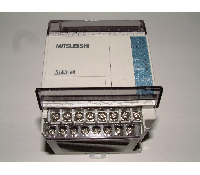
PLC Rack

What makes a PLC special? PLC's are used to automate machinery in assembly lines. For our project, we use the computer link feature that allows a PLC to take commands and communicate with a host computer. If something goes wrong with the computer link, the PLC still functions and protecting valuable equipment.
High Resolution Fly's Eye experiment, uses a Toshiba T1 PLC as part of a steerable laser system used for monitoring atmospheric clarity. We use a model TDR116-6S. The PLC was purchased as part of a starter kit. Specifically the PLC is used to open and close a cover that protects the a steering mechanism when the systems is not used. It is programmed to automatically close this cover after one hour unless it has received and instruction from the main PC to keep the cover open. This means that even if the PC or network communication to the site fails, the cover will still close. It is also used to power cycle equipment, including the laser and the radiometer.
This PLC and most others use a language called relay ladder logic programming. However, if you've programmed in high level languages before don't be fooled by that last part. Ladder logic is not necessarily difficult. Once you get the hang of it it isn't hard at all. But.. ladder logic is quite different from more common programming languages such as FORTRAN or c. It's true that ladder logic uses conditional statements, subroutines and FOR NEXT loops but there are some very significant differences.
Unlike FORTRAN or c, with ladder logic, every 'rung' of the code is multithreaded. Normally in a programming language things happen in order. The command or line of code on top is executed before the command on the bottom until you hit the end of a loop. This is not so in ladder logic. Everything happens at the same time.
So what is ladder logic programming really like? Ladder logic programming looks, well, like a ladder. It's more like a flow chart than a program. There are two vertical lines coming down the programming environment, one on the left and one on the right. Then, you have rungs of conditionals on the left that lead to outputs on the right. For example:
x0001 x0002 Y0001
|---| |-----|/|---------( )-----|
| |
| |
| x0001 Y002 |
|---| |--[01000 TON T012]--( )--|
| |
| |
| R001 |
|--[D0140 = 0001]--------( )--|
| |
| R001 Y004 |
|--| |---------------------( )--|
| |
|-{END}-------------------------|
In Ladder logic programming you do not have variables, you have registers. There are four kinds of registers: X's that are inputs, Y's that are outputs, D's that are data that can form interger, hex and real numbers, and finally R's that are internal relays. X's and Y's are pointers to the actual terminal strip connectors (what you use a screw driver on to connect wires) on the PLC. If you energize an input, let's say 5, then X0005 will have an on status; also if you give Y0023 an on status then relay 23 will flick on. R's are just about the same as X's and Y's except that they don't point to any hardware. They just hold an on or off value inside of the PLC's memory. R's can be useful. X's Y's and R's can even hold data besides their on and off states on many PLC's, but personally I don't recommend it. For data like integers and hexadecimal numbers D's are used as their addresses.
example one. The things you will probably use the most writing Ladder Logic are the relay conditionals --| |-- ---|/|--- and the output coils ---( )---. These three things basically make up a kind of IF THEN statement. This --| |-- means closed if energized while --|/|-- means closed if not energized. The output coil --( )-- basically means then energize this. So the first rung of example one means that if input 1 is energized and input 2 is not then energize output 1. You should note that on the T1, the number of a particular input or output is written on the case of the PLC but for T2's and for some other more advanced PLC's this is not necessarily the case. To find out what the addresses of your inputs and outputs are you should refer to the documentation that came with your PLC. Also, in most ladder logic programming environments you have to specify the address of each of your inputs and outputs before it will even let you start programming. [the T series can auto configure]
delay timer. What this means is that after a specified amount of time after x0001 turns on, y0002 will turn on. You should note that because of the nature of ladder logic you can not simply put a timer attached directly to the left hand side without a relay conditional between it. Remember, everything is happening at the same time. PLC's are meant to run on their own for long periods of time, so you can't just tell it that 10 seconds after it's first plugged in it should activate something. You have to tell it to start timing after something in the outside world has occurred, like the energizing or de-energizing of an input.
In the code --[01000 TON T012]-- there is the parameter 01000 that tells the timer to wait 1000*10ms or 10 seconds, and the parameter T012 tells the PLC which internal timer you want to use. Some of the more advanced PLC's have timers with different accuracy. Most measure time in 10ms intervals but others measure time in single milliseconds. You should check the documentation on your PLC to see if any of it's timers measure time in different units than the others. Also you should not use the same timer for more than one thing.
On rung three of the ladder we have a conditional statement. If the number stored in D0140 is equal to 1 then energize R001. If you look at the entire circuit you'll note that there is no where else in it where D0140 is mentioned and you should know that all data registers are set to 0 at default. You may think that D0140 will never actually reach the value of 1 and that R001 will never be activated and that rung three and four are useless garbage code. It's true that during the normal operation of the PLC D0140 will never change from zero and the last two rungs before end would be useless. However, this is where the computer link function comes in. All Toshiba PLC's have a computer link protocol built into them. This allows a host computer, such as any sort of DOS, Linux based PC or even a Unix administrator with an RS232 serial port to send commands to the PLC while it's running and read or write values into its registers. This includes data, inputs, outputs, and relays.
Suppose that Y004 was attached to equipment that you wanted to turn it on or off at your pleasure. Suppose it was an air conditioner or maybe some strange contraption that brought you a coke from the fridge to your seat at a computer. If you can write a program at your own specialized system that can send ASCII characters with 8 data bits 1 start bit 1 stop bit and 9600 baud rate with odd parity, then you can manipulate the registers in the Toshiba PLC's and toggle d0140 between 1 and zero or 1 and any other value. See more about the computer link function with a sample C program written under Linux latter. C example
The final rung on the ladder the -{END}- is basically what it says. It's the end statement. It doesn't really do anything except to say, well, your done programming. However, no program will work without an end statement and the PLC will ignore any code put in after an end statement. This shouldn't be a problem for small programs, just look at the screen and make sure the end is in there and at the bottom. If you happen to be making a very large and a very complicated relay circuit your editor will likely force you to write it in separate blocks. Before attempting to write a very large program you should go to the very last programming block available to you and put the end statement there and no where else. The end statement can be used in debugging by ending the program early and disabling commands that fall after the end statement.
| X001 Y001 Y001 |
|-| |---|/|---[01000 TON T002]-[01000 TOF T003]---------( )--| rung one
| |
| X001 Y002 |
|--| |----+---------------------------------------------( )--| rung two
| | |
| Y002 | |
|--| |----+ |
| X001 R006 |
|--| |--|/|--[01000 TON T004]-----+-------[D150 + 1 -> D150]-| rung three
| | R006 |
| +---[01000 TOF T005]--( )--|
| |
| Y003 |
|-[D150 >200]-------------------------------------------( )--| rung four
| |
| Y003 |
|-| |-----------------------------------------[ 0 MOV D150]--| rung five
| |
|--{END}-----------------------------------------------------| END rung
Example two is a bit more complicated than example one, but once you understand it you'll be on your way to being able to design your own relay ladder logic. Rung one is especially interesting. A TON and a TOF combination that lets output Y001 cycle on and off for 10 seconds at a time. While TON waits a given time before allowing an energized input to affect an output, TOF waits a given time before de-energizing an output after it's input has been cut off.
Let's analyze the rung. The -| |- conditional with X001 is there for good programming, it isn't actually necessary in this rung but if it's not there you have no way to stop the oscillating of Y001 during the PLC's operation. Now notice that we're not allowing current to flow if Y001 is energized yet the output of this rung is to energize Y001. Well, if Y001 is off then current is passed to TON. After TON has gone through it's specified time it will energize Y001. Now that Y001 is energized current to the rung is cut off. Once the current has stopped TOF will keep Y001 powered for a specified amount of time before Y001 feels the affects and de-energizes. With Y001 de-energized TON is energized again and the cycle goes on. (You may want to reread that last sentence a few times) The output Y001 stays on for a second, then off for a second continuously cycling.
Rung two shows how to set up a push button. With a momentary push button, the input is only energized for a short amount of time, but often it is useful to keep the rung on long afterwards. What you should notice about rung two is that the output is connected to the left hand side twice. If either of the two relay conditionals are on, then the output is on. Notice that one of the relay conditionals is the output itself. Thus if the output is powered for just one of the PLC's cycles (a very short time) then the output's own momentary on state will keep itself energized. You want to put in an internal relay conditional between the Y002 input and output or else you'll never be able to get it off! Well you could if you restart the PLC's program or with the computer link protocol.
Rung three is also spread across two rung slots but you could get it on one rung if it would fit ( it really doesn't all fit on one rung in the editor). It's basically like rung one except that between the timers is a data statement that increments D150 by one. There are other ways to increment a data register, but this is what I used. Because it's between the timers, the data function will only get power and operate once during the period of the cycle. Since most of the timers only measure in milliseconds you can use a rung like this to measure time in hours or days if your PLC doesn't have any function that will do it for you.
Rung four simply turns on an output when D150 is greater than a number i.e. a certain amount of time has gone by.
Rung five sets D150 back to 0 when that output has been on momentarily. In a real application of something like this you'd probably want to use a TOF on rung four so that when D150 is no longer greater than 200 Y003 will wait a moment before deactivating, other wise it will deactivate after one cycle of the PLC. The PLC probably goes through around a thousand cycles per second. A cycle is when the PLC updates the on, off, and value states of the relays and registers.
You should notice that I didn't just say D150=0. The = sign is already used in conditionals so instead you have to use a move command. The --[0 MOV D150]-- means move the value of 0 into the register D150. There are many other data functions and ladder logic components that you can use. So far I've only gone over what I think are the most important ones. For example, the T1 also haws its own counters and flip flop's built in to use in your program. Don't be afraid to experiment for your self though. When you buy the starter kit a you get PLC, a ladder logic editor and documentation including a list of all of the programming components, hardware, and exactly how everything works.
http://xtronics.com/toshiba/Ladder_logic.htm
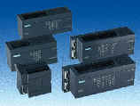
PLC pic :
PLC Rack
Monday, August 6, 2007
Advanced Micro Devices
From Wikipedia, the free encyclopedia

Advanced Micro Devices, Inc. (abbreviated AMD; NYSE: AMD) is an American manufacturer of semiconductors based in Sunnyvale, California. The company was founded in 1969 by a group of former executives from Fairchild Semiconductor, including Jerry Sanders, III, Ed Turney, John Carey, Sven Simonsen, Jack Gifford and three members from Gifford's team, Frank Botte, Jim Giles and Larry Stenger. The current chairman and CEO is Dr. Héctor Ruiz and the current president and chief operating officer is Dirk Meyer.
AMD is the world's second-largest supplier of x86 based processors and the world's second largest supplier of graphics cards and GPUs, after taking control over ATI in 2006. AMD also owns a 37% share of Spansion, a supplier of non-volatile flash memory. In 2006 the company ranked eighth among semiconductor manufacturers.
General history

Early AMD 8080 Processor (AMD AM9080ADC / C8080A), 1977
AMD started as a producer of logic chips in 1969, then entered the RAM chip business in 1975. That same year, it introduced a reverse-engineered clone of the Intel 8080 microprocessor. During this period, AMD also designed and produced a series of bit-slice processor elements (Am2900, Am29116, Am293xx) which were used in various minicomputer designs.
During this time, AMD attempted to embrace the perceived shift towards RISC with their own AMD 29K processor, and they attempted to diversify into graphics and audio devices as well as EPROM memory. It had some success in the mid-80s with the AMD7910 and AMD7911 "World Chip" FSK modem, one of the first multistandard devices that covered both Bell and CCITT tones at up to 1200 baud half duplex or 300/300 full duplex. While the AMD 29K survived as an embedded processor and AMD spinoff Spansion continues to make industry leading flash memory, AMD was not as successful with its other endeavors. AMD decided to switch gears and concentrate solely on Intel-compatible microprocessors and flash memory. This put them in direct competition with Intel for x86 compatible processors and their flash memory secondary markets.
Litigation with Intel
AMD has a long history of litigation with former partner and x86 creator Intel.
• In 1986 Intel broke an agreement it had with AMD to allow them to produce Intel's micro-chips for IBM; AMD filed for arbitration in 1987 and the arbitrator decided in AMD's favor in 1992. Intel disputed this, and the case ended up in the Supreme Court of California. In 1994, that court upheld the arbitrator's decision and awarded damages for breach of contract.
• In 1990, Intel brought a copyright infringement action alleging illegal use of its 287 microcode. The case ended in 1994 with a jury finding for AMD and its right to use Intel's microcode in its microprocessors through the 486 generation.
• In 1997, Intel filed suit against AMD and Cyrix Corp. for misuse of the term MMX. AMD and Intel settled, with AMD acknowledging MMX as a trademark owned by Intel, and with Intel granting AMD rights to market the AMD K6 MMX processor.
• In 2005, following an investigation, the Japan Federal Trade Commission found Intel guilty on a number of violations. On June 27, 2005, AMD won an antitrust suit against Intel in Japan, and on the same day, AMD filed a broad antitrust complaint against Intel in the U.S. Federal District Court in Delaware. The complaint alleges systematic use of secret rebates, special discounts, threats, and other means used by Intel to lock AMD processors out of the global market. Since the start of this action, AMD has issued subpoenas to major computer manufacturers including Dell, Microsoft, IBM, HP, Sony, and Toshiba.
Merger with ATI
AMD announced a merger with ATI Technologies on July 24, 2006. AMD had paid $4.2 billion in cash along with 57 million shares of its stock, for a total of a US$5.4 billion. The merger had completed on October 25, 2006[4] and ATI is now part of AMD.
It has been reported that in December 2006 AMD received a subpoena from the Justice Department regarding possible antitrust violations relating to the merger.
AMD x86 processors
Discontinued
8086, Am286, Am386, Am486, Am5x86

AMD 80286 1982
In February 1982, AMD signed a contract with Intel, becoming a licensed second-source manufacturer of 8086 and 8088 processors. IBM wanted to use the Intel 8088 in its IBM PC, but IBM's policy at the time was to require at least two sources for its chips. AMD later produced the Am286 under the same arrangement, but Intel canceled the agreement in 1986 and refused to convey technical details of the i386 part.
AMD challenged Intel's decision to cancel the agreement and won in arbitration, but Intel disputed this decision. A long legal dispute followed, ending in 1994 when the Supreme Court of California sided with AMD. Subsequent legal disputes centered on whether AMD had legal rights to use derivatives of Intel's microcode. In the face of uncertainty, AMD was forced to develop "clean room" versions of Intel code.
In 1991, AMD released the Am386, its clone of the Intel 386 processor. It took less than a year for the company to sell a million units. Later, the Am486 was used by a number of large OEMs, including Compaq, and proved popular. Another Am486-based product, the Am5x86, continued AMD's success as a low-price alternative. However, as product cycles shortened in the PC industry, the process of reverse engineering Intel's products became an ever less viable strategy for AMD.
K5, K6, Athlon (K7)
AMD's first completely in-house x86 processor was the K5 which was launched in 1996.[6] The "K" was a reference to "Kryptonite", which from comic book lore, was the only substance that could harm Superman, with a clear reference to Intel, which dominated in the market at the time, as "Superman" .[7]
In 1996, AMD purchased NexGen specifically for the rights to their Nx series of x86-compatible processors. AMD gave the NexGen design team their own building, left them alone, and gave them time and money to rework the Nx686. The result was the K6 processor, introduced in 1997.
The K7 was AMD's seventh generation x86 processor, making its debut on June 23, 1999, under the brand name Athlon.
Current and future
Athlon 64 (K8)
The K8 is a major revision of the K7 architecture, with the most notable features being the addition of a 64-bit extension to the x86 instruction set (officially called AMD64), the incorporation of an on-chip memory controller, and the implementation of an extremely high performance point-to-point interconnect called HyperTransport, as part of the Direct Connect Architecture. The technology was initially launched as the Opteron server-oriented processor.[8] Shortly thereafter it was incorporated into a product for desktop PCs, branded Athlon 64.
Dual-core Athlon 64 X2

AMD released the first dual core Opteron, an x86-based server CPU, on April 21, 2005.[10] The first desktop-based dual core processor family — the Athlon 64 X2 came a month later.

Quad-core "Barcelona" die-shot
In early May, AMD had abandoned the string "64" in its dual-core desktop product branding, becoming Athlon X2, while upcoming updates involves some of the improvements to the microarchitecture, and a shift of target market from mainstream desktop systems to value dual-core desktop systems, to avoid conflict of target customers between another dual-core product based on the K10 microarchitecture, the Phenom X2.
K10
The latest microprocessor architecture, also known as "AMD K10" is AMD's new microarchitecture. The "AMD K10" microarchitecture is the immediate successor to the AMD K8 microarchitecture, and is expected due middle of 2007. K10 processors will come in a single, dual, and quad-core versions with all cores on one single die.
Bulldozer and Bobcat
After the K10 architecture, AMD will move to a modular design methodology named "M-SPACE", where two new processor cores, codenamed "Bulldozer" and "Bobcat" will be released in the 2009 timeframe. While very little prelimilary information exists even in AMD's Technology Analyst Day 2007, both cores are to be built from the ground up. The Bulldozer core focused on 10 Watts to 100 Watts products, with optimizations for performance-per-watt ratios and HPC applications, while the Bobcat core will focus on 1 Watt to 10 Watts products, given that the core is a simplified x86 core to reduce power draw. Both of the cores will be able to corporate with full DirectX compatible GPU core(s) under the Fusion label.
AMD Fusion
After the merger between AMD and ATI, an initiative codenamed Fusion was announced that merges a CPU and GPU on one chip, including a minimum 16 lane PCI Express link to accommodate external PCI Express peripherals, thereby eliminating the requirement of a northbridge chip completely from the motherboard. It is expected to be released in 2009, one of the fruits of Fusion is the codenamed Falcon family, implementing the codenamed Bulldozer core, aimed for a 10-100 W products, and further products will incorporate codenamed Bobcat core, focusing on sub-10 W markets, targeting UMPC products and small handheld devices which was widely adopted the ARM processors. Processors from this project, will also be deployed in notebooks, with quad-core processors planned for 2009 reelase.
Other platforms and technologies
AMD Live!

AMD LIVE! is a platform marketing initiative focusing the consumer electronics segment, with a recently announced Active TV initiative for streaming Internet videos from web video services such as YouTube, into AMD Live! PC as well as connected digital TVs, together with a scheme for an ecosystem of certified peripherals for the ease of customers to identify peripherals for AMD Live! systems for digital home experience, called "AMD Live! Ready".
AMD Quad FX platform
The AMD Quad FX platform, being an extreme enthusiast platform, allows two processors connect through HyperTransport, which is a similar setup to dual-processor (2P) servers, excluding the use of buffered memory/registered memory DIMM modules, and a server motherboard, the current setup includes two Athlon 64 FX FX-70 series processors and a special motherboard. AMD pushed the platform for the surging demands for what AMD calls "megatasking" for true enthusiasts[citation needed], the ability to do more tasks on one single system. The platform refreshes with the introduction of Phenom FX processors and the next-generation RD790 chipset, codenamed "FASN8".
Commercial platform
Virtualization
AMD's virtualization extension to the 64-bit x86 architecture is named AMD Virtualization, also known by the abbreviation AMD-V, and is sometimes referred to by the code name "Pacifica". AMD processors using Socket AM2, Socket S1, and Socket F include AMD Virtualization support. AMD Virtualization is also supported by release two (8200, 2200 and 1200 series) of the Opteron processors.
AMD also endorsed the development of I/O virtualization technology, currently the "AMD I/O Virtualization Technology" (also known as IOMMU) specification published using HyperTransport architecture by AMD had updated to version 1.2 [13][14], which the first finalized (version 1.0) specification was published prior to Intel's[citation needed].
Commercial initiatives
• AMD Trinity, provides support for virtualization, security and management. Key features include AMD-V technology, codenamed Presidio trusted computing platform technology, I/O Virtualization and Open Management Partition. [15]
• AMD Raiden, future clients similar to the Jack PC [16] to be connected through network to a blade server for central management, to reduce client form factor sizes with AMD Trinity features.
• Torrenza, co-processors support through interconnects such as HyperTransport as PCI Express (though more focus was at HyperTransport enabled co-processors), also opening processor socket architecture to other manufacturers, Sun and IBM are among the supporting consortium, with rumoured POWER7 processors would be socket-compatible to future Opteron processors. The move made rival Intel responded with the open of Front Side Bus (FSB) architecture as well as Geneseo [17], a collaboration project with IBM for co-processors connected through PCI Express. Note that AMD positioned Torrenza for commercial segment, whilst Intel positioned Geneseo for all segments including consumer desktop segments[citation needed].
• Various certified systems programs and platforms: AMD Commercial Stable Image Platform (CSIP), together with AMD Validated Server program, AMD True Server Solutions, AMD Thermally Tested Barebones Platforms and AMD Validated Server Program, providing certified systems for business from AMD.
Desktop platforms
Starting from 2007, AMD has also following Intel, to use codenames for each desktop platforms. The platforms, unlike Intel's approach, will refresh every year, putting focus on platform specialization. The platform includes components as AMD processors, chipsets, ATI graphics and other features, but continued to the open platform approach, and welcome components from other vendors such as VIA, SiS, and NVIDIA, as well as wireless product vendors.
AMD will also release a system controls utility in the future, providing easy system monitoring, allowing adjustments to voltages and clocks, as well as overall platform management, including CPU, chipset and graphics. The features are expected to be similar to the control panel in NVIDIA ForceWare series drivers.
Embedded systems
Alchemy Processors
In February 2002, AMD acquired Alchemy Semiconductor and continued its line of processor in MIPS architecture processors, targets the handheld and Portable media player markets. On 13 June 2006, AMD officially announced that the Alchemy processor line was transferred to Raza Microelectronics Inc.
Geode processors
In August 2003, AMD also purchased the Geode business which was originally the Cyrix MediaGX from National Semiconductor to augment its existing line of embedded x86 processor products. During the second quarter of 2004, it launched new low-power Geode NX processors based on the K7 Thoroughbred architecture with speeds of fanless processors 667 MHz and 1 GHz, and 1.4 GHz processor with fan, of TDP 25 W.
Flash technology
While less visible to the general public than its CPU business, AMD is also a global leader in flash memory. In 1993, AMD established a 50-50 partnership with Fujitsu called FASL, and merged into a new company called FASL LLC in 2003. The joint venture firm went public under ticker symbol SPSN in December 2005, with AMD shares drop to 37%.
AMD no longer directly participates in the Flash memory devices market now as AMD entered into a non-competition agreement, as of December 21, 2005, with Fujitsu and Spansion, pursuant to which it agreed not to directly or indirectly engage in a business that manufactures or supplies standalone semiconductor devices (including single chip, multiple chip or system devices) containing only Flash memory [19].
Mobile platforms

AMD started a platform in 2003 aimed at mobile computing, but with fewer advertisements and promotional schemes, very little was known about the platform. The platform used mobile Athlon 64 or mobile Sempron processors.
As part of the "Better by design" initiative, the open mobile platform, announced February 2007 with announcement of general availability in May 2007, comes together with 65 nm fabrication process Turion 64 X2, and is consists of three major components, as AMD processor, graphics from either NVIDIA or ATI Technologies which also includes integrated graphics (IGP), and wireless connectivity solutions from Atheros, Broadcom, Marvell, Qualcomm or Realtek.
Upcoming platforms were being discussed with Puma platform and Griffin processor to be released in 2008. AMD planned quad-core processors with 3D graphics capcabilities (Fusion) to be launched in 2009 with the Eagle platform.
Advanced Micro Devices, Inc. (abbreviated AMD; NYSE: AMD) is an American manufacturer of semiconductors based in Sunnyvale, California. The company was founded in 1969 by a group of former executives from Fairchild Semiconductor, including Jerry Sanders, III, Ed Turney, John Carey, Sven Simonsen, Jack Gifford and three members from Gifford's team, Frank Botte, Jim Giles and Larry Stenger. The current chairman and CEO is Dr. Héctor Ruiz and the current president and chief operating officer is Dirk Meyer.
AMD is the world's second-largest supplier of x86 based processors and the world's second largest supplier of graphics cards and GPUs, after taking control over ATI in 2006. AMD also owns a 37% share of Spansion, a supplier of non-volatile flash memory. In 2006 the company ranked eighth among semiconductor manufacturers.
General history

Early AMD 8080 Processor (AMD AM9080ADC / C8080A), 1977
AMD started as a producer of logic chips in 1969, then entered the RAM chip business in 1975. That same year, it introduced a reverse-engineered clone of the Intel 8080 microprocessor. During this period, AMD also designed and produced a series of bit-slice processor elements (Am2900, Am29116, Am293xx) which were used in various minicomputer designs.
During this time, AMD attempted to embrace the perceived shift towards RISC with their own AMD 29K processor, and they attempted to diversify into graphics and audio devices as well as EPROM memory. It had some success in the mid-80s with the AMD7910 and AMD7911 "World Chip" FSK modem, one of the first multistandard devices that covered both Bell and CCITT tones at up to 1200 baud half duplex or 300/300 full duplex. While the AMD 29K survived as an embedded processor and AMD spinoff Spansion continues to make industry leading flash memory, AMD was not as successful with its other endeavors. AMD decided to switch gears and concentrate solely on Intel-compatible microprocessors and flash memory. This put them in direct competition with Intel for x86 compatible processors and their flash memory secondary markets.
Litigation with Intel
AMD has a long history of litigation with former partner and x86 creator Intel.
• In 1986 Intel broke an agreement it had with AMD to allow them to produce Intel's micro-chips for IBM; AMD filed for arbitration in 1987 and the arbitrator decided in AMD's favor in 1992. Intel disputed this, and the case ended up in the Supreme Court of California. In 1994, that court upheld the arbitrator's decision and awarded damages for breach of contract.
• In 1990, Intel brought a copyright infringement action alleging illegal use of its 287 microcode. The case ended in 1994 with a jury finding for AMD and its right to use Intel's microcode in its microprocessors through the 486 generation.
• In 1997, Intel filed suit against AMD and Cyrix Corp. for misuse of the term MMX. AMD and Intel settled, with AMD acknowledging MMX as a trademark owned by Intel, and with Intel granting AMD rights to market the AMD K6 MMX processor.
• In 2005, following an investigation, the Japan Federal Trade Commission found Intel guilty on a number of violations. On June 27, 2005, AMD won an antitrust suit against Intel in Japan, and on the same day, AMD filed a broad antitrust complaint against Intel in the U.S. Federal District Court in Delaware. The complaint alleges systematic use of secret rebates, special discounts, threats, and other means used by Intel to lock AMD processors out of the global market. Since the start of this action, AMD has issued subpoenas to major computer manufacturers including Dell, Microsoft, IBM, HP, Sony, and Toshiba.
Merger with ATI
AMD announced a merger with ATI Technologies on July 24, 2006. AMD had paid $4.2 billion in cash along with 57 million shares of its stock, for a total of a US$5.4 billion. The merger had completed on October 25, 2006[4] and ATI is now part of AMD.
It has been reported that in December 2006 AMD received a subpoena from the Justice Department regarding possible antitrust violations relating to the merger.
AMD x86 processors
Discontinued
8086, Am286, Am386, Am486, Am5x86

AMD 80286 1982
In February 1982, AMD signed a contract with Intel, becoming a licensed second-source manufacturer of 8086 and 8088 processors. IBM wanted to use the Intel 8088 in its IBM PC, but IBM's policy at the time was to require at least two sources for its chips. AMD later produced the Am286 under the same arrangement, but Intel canceled the agreement in 1986 and refused to convey technical details of the i386 part.
AMD challenged Intel's decision to cancel the agreement and won in arbitration, but Intel disputed this decision. A long legal dispute followed, ending in 1994 when the Supreme Court of California sided with AMD. Subsequent legal disputes centered on whether AMD had legal rights to use derivatives of Intel's microcode. In the face of uncertainty, AMD was forced to develop "clean room" versions of Intel code.
In 1991, AMD released the Am386, its clone of the Intel 386 processor. It took less than a year for the company to sell a million units. Later, the Am486 was used by a number of large OEMs, including Compaq, and proved popular. Another Am486-based product, the Am5x86, continued AMD's success as a low-price alternative. However, as product cycles shortened in the PC industry, the process of reverse engineering Intel's products became an ever less viable strategy for AMD.
K5, K6, Athlon (K7)
AMD's first completely in-house x86 processor was the K5 which was launched in 1996.[6] The "K" was a reference to "Kryptonite", which from comic book lore, was the only substance that could harm Superman, with a clear reference to Intel, which dominated in the market at the time, as "Superman" .[7]
In 1996, AMD purchased NexGen specifically for the rights to their Nx series of x86-compatible processors. AMD gave the NexGen design team their own building, left them alone, and gave them time and money to rework the Nx686. The result was the K6 processor, introduced in 1997.
The K7 was AMD's seventh generation x86 processor, making its debut on June 23, 1999, under the brand name Athlon.
Current and future
Athlon 64 (K8)
The K8 is a major revision of the K7 architecture, with the most notable features being the addition of a 64-bit extension to the x86 instruction set (officially called AMD64), the incorporation of an on-chip memory controller, and the implementation of an extremely high performance point-to-point interconnect called HyperTransport, as part of the Direct Connect Architecture. The technology was initially launched as the Opteron server-oriented processor.[8] Shortly thereafter it was incorporated into a product for desktop PCs, branded Athlon 64.
Dual-core Athlon 64 X2
AMD released the first dual core Opteron, an x86-based server CPU, on April 21, 2005.[10] The first desktop-based dual core processor family — the Athlon 64 X2 came a month later.

Quad-core "Barcelona" die-shot
In early May, AMD had abandoned the string "64" in its dual-core desktop product branding, becoming Athlon X2, while upcoming updates involves some of the improvements to the microarchitecture, and a shift of target market from mainstream desktop systems to value dual-core desktop systems, to avoid conflict of target customers between another dual-core product based on the K10 microarchitecture, the Phenom X2.
K10
The latest microprocessor architecture, also known as "AMD K10" is AMD's new microarchitecture. The "AMD K10" microarchitecture is the immediate successor to the AMD K8 microarchitecture, and is expected due middle of 2007. K10 processors will come in a single, dual, and quad-core versions with all cores on one single die.
Bulldozer and Bobcat
After the K10 architecture, AMD will move to a modular design methodology named "M-SPACE", where two new processor cores, codenamed "Bulldozer" and "Bobcat" will be released in the 2009 timeframe. While very little prelimilary information exists even in AMD's Technology Analyst Day 2007, both cores are to be built from the ground up. The Bulldozer core focused on 10 Watts to 100 Watts products, with optimizations for performance-per-watt ratios and HPC applications, while the Bobcat core will focus on 1 Watt to 10 Watts products, given that the core is a simplified x86 core to reduce power draw. Both of the cores will be able to corporate with full DirectX compatible GPU core(s) under the Fusion label.
AMD Fusion
After the merger between AMD and ATI, an initiative codenamed Fusion was announced that merges a CPU and GPU on one chip, including a minimum 16 lane PCI Express link to accommodate external PCI Express peripherals, thereby eliminating the requirement of a northbridge chip completely from the motherboard. It is expected to be released in 2009, one of the fruits of Fusion is the codenamed Falcon family, implementing the codenamed Bulldozer core, aimed for a 10-100 W products, and further products will incorporate codenamed Bobcat core, focusing on sub-10 W markets, targeting UMPC products and small handheld devices which was widely adopted the ARM processors. Processors from this project, will also be deployed in notebooks, with quad-core processors planned for 2009 reelase.
Other platforms and technologies
AMD Live!

AMD LIVE! is a platform marketing initiative focusing the consumer electronics segment, with a recently announced Active TV initiative for streaming Internet videos from web video services such as YouTube, into AMD Live! PC as well as connected digital TVs, together with a scheme for an ecosystem of certified peripherals for the ease of customers to identify peripherals for AMD Live! systems for digital home experience, called "AMD Live! Ready".
AMD Quad FX platform
The AMD Quad FX platform, being an extreme enthusiast platform, allows two processors connect through HyperTransport, which is a similar setup to dual-processor (2P) servers, excluding the use of buffered memory/registered memory DIMM modules, and a server motherboard, the current setup includes two Athlon 64 FX FX-70 series processors and a special motherboard. AMD pushed the platform for the surging demands for what AMD calls "megatasking" for true enthusiasts[citation needed], the ability to do more tasks on one single system. The platform refreshes with the introduction of Phenom FX processors and the next-generation RD790 chipset, codenamed "FASN8".
Commercial platform
Virtualization
AMD's virtualization extension to the 64-bit x86 architecture is named AMD Virtualization, also known by the abbreviation AMD-V, and is sometimes referred to by the code name "Pacifica". AMD processors using Socket AM2, Socket S1, and Socket F include AMD Virtualization support. AMD Virtualization is also supported by release two (8200, 2200 and 1200 series) of the Opteron processors.
AMD also endorsed the development of I/O virtualization technology, currently the "AMD I/O Virtualization Technology" (also known as IOMMU) specification published using HyperTransport architecture by AMD had updated to version 1.2 [13][14], which the first finalized (version 1.0) specification was published prior to Intel's[citation needed].
Commercial initiatives
• AMD Trinity, provides support for virtualization, security and management. Key features include AMD-V technology, codenamed Presidio trusted computing platform technology, I/O Virtualization and Open Management Partition. [15]
• AMD Raiden, future clients similar to the Jack PC [16] to be connected through network to a blade server for central management, to reduce client form factor sizes with AMD Trinity features.
• Torrenza, co-processors support through interconnects such as HyperTransport as PCI Express (though more focus was at HyperTransport enabled co-processors), also opening processor socket architecture to other manufacturers, Sun and IBM are among the supporting consortium, with rumoured POWER7 processors would be socket-compatible to future Opteron processors. The move made rival Intel responded with the open of Front Side Bus (FSB) architecture as well as Geneseo [17], a collaboration project with IBM for co-processors connected through PCI Express. Note that AMD positioned Torrenza for commercial segment, whilst Intel positioned Geneseo for all segments including consumer desktop segments[citation needed].
• Various certified systems programs and platforms: AMD Commercial Stable Image Platform (CSIP), together with AMD Validated Server program, AMD True Server Solutions, AMD Thermally Tested Barebones Platforms and AMD Validated Server Program, providing certified systems for business from AMD.
Desktop platforms
Starting from 2007, AMD has also following Intel, to use codenames for each desktop platforms. The platforms, unlike Intel's approach, will refresh every year, putting focus on platform specialization. The platform includes components as AMD processors, chipsets, ATI graphics and other features, but continued to the open platform approach, and welcome components from other vendors such as VIA, SiS, and NVIDIA, as well as wireless product vendors.
AMD will also release a system controls utility in the future, providing easy system monitoring, allowing adjustments to voltages and clocks, as well as overall platform management, including CPU, chipset and graphics. The features are expected to be similar to the control panel in NVIDIA ForceWare series drivers.
Embedded systems
Alchemy Processors
In February 2002, AMD acquired Alchemy Semiconductor and continued its line of processor in MIPS architecture processors, targets the handheld and Portable media player markets. On 13 June 2006, AMD officially announced that the Alchemy processor line was transferred to Raza Microelectronics Inc.
Geode processors
In August 2003, AMD also purchased the Geode business which was originally the Cyrix MediaGX from National Semiconductor to augment its existing line of embedded x86 processor products. During the second quarter of 2004, it launched new low-power Geode NX processors based on the K7 Thoroughbred architecture with speeds of fanless processors 667 MHz and 1 GHz, and 1.4 GHz processor with fan, of TDP 25 W.
Flash technology
While less visible to the general public than its CPU business, AMD is also a global leader in flash memory. In 1993, AMD established a 50-50 partnership with Fujitsu called FASL, and merged into a new company called FASL LLC in 2003. The joint venture firm went public under ticker symbol SPSN in December 2005, with AMD shares drop to 37%.
AMD no longer directly participates in the Flash memory devices market now as AMD entered into a non-competition agreement, as of December 21, 2005, with Fujitsu and Spansion, pursuant to which it agreed not to directly or indirectly engage in a business that manufactures or supplies standalone semiconductor devices (including single chip, multiple chip or system devices) containing only Flash memory [19].
Mobile platforms

AMD started a platform in 2003 aimed at mobile computing, but with fewer advertisements and promotional schemes, very little was known about the platform. The platform used mobile Athlon 64 or mobile Sempron processors.
As part of the "Better by design" initiative, the open mobile platform, announced February 2007 with announcement of general availability in May 2007, comes together with 65 nm fabrication process Turion 64 X2, and is consists of three major components, as AMD processor, graphics from either NVIDIA or ATI Technologies which also includes integrated graphics (IGP), and wireless connectivity solutions from Atheros, Broadcom, Marvell, Qualcomm or Realtek.
Upcoming platforms were being discussed with Puma platform and Griffin processor to be released in 2008. AMD planned quad-core processors with 3D graphics capcabilities (Fusion) to be launched in 2009 with the Eagle platform.
Sunday, August 5, 2007
Programmable logic controller
From Wikipedia, the free encyclopedia
A Programmable Logic Controller, PLC, or Programmable Controller is a digital computer used for automation of industrial processes, such as control of machinery on factory assembly lines. Unlike general-purpose computers, the PLC is designed for multiple inputs and output arrangements, extended temperature ranges, immunity to electrical noise, and resistance to vibration and impact. Programs to control machine operation are typically stored in battery-backed or non-volatile memory. A PLC is an example of a real time system since output results must be produced in response to input conditions within a bounded time, otherwise unintended operation will result.
Features
The main difference from other computers is that PLC are armored for severe condition (dust, moisture, heat, cold, etc) and have the facility for extensive input/output (I/O) arrangements. These connect the PLC to sensors and actuators. PLCs read limit switches, analog process variables (such as temperature and pressure), and the positions of complex positioning systems. Some even use machine vision. On the actuator side, PLCs operate electric motors, pneumatic or hydraulic cylinders, magnetic relays or solenoids, or analog outputs. The input/output arrangements may be built into a simple PLC, or the PLC may have external I/O modules attached to a computer network that plugs into the PLC.
PLCs were invented as replacements for automated systems that would use hundreds or thousands of relays, cam timers, and drum sequencers. Often, a single PLC can be programmed to replace thousands of relays. Programmable controllers were initially adopted by the automotive manufacturing industry, where software revision replaced the re-wiring of hard-wired control panels when production models changed.
Many of the earliest PLCs expressed all decision making logic in simple ladder logic which appeared similar to electrical schematic diagrams. The electricians were quite able to trace out circuit problems with schematic diagrams using ladder logic. This program notation was chosen to reduce training demands for the existing technicians. Other early PLCs used a form of instruction list programming, based on a stack-based logic solver.
The functionality of the PLC has evolved over the years to include sequential relay control, motion control, process control, distributed control systems and networking. The data handling, storage, processing power and communication capabilities of some modern PLCs are approximately equivalent to desktop computers. PLC-like programming combined with remote I/O hardware, allow a general-purpose desktop computer to overlap some PLCs in certain applications.
Under the IEC 61131-3 standard, PLCs can be programmed using standards-based programming languages. A graphical programming notation called Sequential Function Charts is available on certain programmable controllers.
PLC compared with other control systems
PLCs are well-adapted to a certain range of automation tasks. These are typically industrial processes in manufacturing where the cost of developing and maintaining the automation system is high relative to the total cost of the automation, and where changes to the system would be expected during its operational life. PLCs contain input and output devices compatible with industrial pilot devices and controls; little electrical design is required, and the design problem centers on expressing the desired sequence of operations in ladder logic (or function chart) notation. PLC applications are typically highly customized systems so the cost of a packaged PLC is low compared to the cost of a specific custom-built controller design. On the other hand, in the case of mass-produced goods, customized control systems are economic due to the lower cost of the components, which can be optimally chosen instead of a "generic" solution, and where the non-recurring engineering charges are spread over thousands of sales.
For high volume or very simple fixed automation tasks, different techniques are used. For example, a consumer dishwasher would be controlled by an electromechanical cam timer costing only a few dollars in production quantities.
A microcontroller-based design would be appropriate where hundreds or thousands of units will be produced and so the development cost (design of power supplies and input/output hardware) can be spread over many sales, and where the end-user would not need to alter the control. Automotive applications are an example; millions of units are built each year, and very few end-users alter the programming of these controllers. However, some specialty vehicles such as transit busses economically use PLCs instead of custom-designed controls, because the volumes are low and the development cost would be uneconomic.
Very complex process control, such as used in the chemical industry, may require algorithms and performance beyond the capability of even high-performance PLCs. Very high-speed or precision controls may also require customized solutions; for example, aircraft flight controls.
PLCs may include logic for single-variable feedback analog control loop, a "proportional, integral, derivative" or "PID controller." A PID loop could be used to control the temperature of a manufacturing process, for example. Historically PLCs were usually configured with only a few analog control loops; where processes required hundreds or thousands of loops, a distributed control system (DCS) would instead be used. However, as PLCs have become more powerful, the boundary between DCS and PLC applications has become less clear-cut.
Digital and analog signals
Digital or discrete signals behave as binary switches, yielding simply an On or Off signal (1 or 0, True or False, respectively). Pushbuttons, limit switches, and photoelectric sensors are examples of devices providing a discrete signal. Discrete signals are sent using either voltage or current, where a specific range is designated as On and another as Off. A PLC might use 24 V DC I/O, with values above 22 V DC representing On and values below 2VDC representing Off. Initially, PLCs had only discrete I/O.
Analog signals are like volume controls, with a range of values between zero and full-scale. These are typically interpreted as integer values (counts) by the PLC, with various ranges of accuracy depending on the device and the number of bits available to store the data. As PLCs typically use 16-bit signed binary processors, the integer values are limited between -32,768 and +32,767. Pressure, temperature, flow, and weight are often represented by analog signals. Analog signals can use voltage or current with a magnitude proportional to the value of the process signal. For example, an analog 4-20 mA or 0 - 10 V input would be converted into an integer value of 0 - 32767.
Current inputs are less sensitive to electrical noise (i.e. from welders or electric motor starts) than voltage inputs.
Example
As an example, say the facility needs to store water in a tank. The water is drawn from the tank by another system, as needed and our example system must manage the water level in the tank.
Using only digital signals, the PLC has two digital inputs from float switches (tank empty and tank full). The PLC uses a digital output to open and close the inlet valve into the tank.
If both float switches are off (down) or only the 'tank empty' switch is on, the PLC will open the valve to let more water in. If only the 'tank full' switch is on, the valve turns off. Both switches being on would signal that something is wrong with one of the switches, as the tank cannot be both full and empty at the same time. Two float switches are used to prevent a 'flutter' condition where any water usage activates the pump for a very short time causing the system to wear out faster.
An analog system might use a load cell (scale) that weighs the tank, and an adjustable (throttling) valve. The PLC could use a PID feedback loop to control the valve opening. The load cell is connected to an analog input and the valve is connected to an analog output. This system fills the tank faster when there is less water in the tank. If the water level drops rapidly, the valve can be opened wide. If water is only dripping out of the tank, the valve adjusts to slowly drip water back into the tank.
In this system, to avoid 'flutter' adjustments that can wear out the valve, many PLCs incorporate "hysteresis" which essentially creates a "deadband" of activity. A technician adjusts this deadband so the valve moves only for a significant change in rate. This will in turn minimize the motion of the valve, and reduce its wear.
A real system might combine both approaches, using float switches and simple valves to prevent spills, and a rate sensor and rate valve to optimize refill rates. Backup and maintenance methods can make a real system very complicated.
System scale
A small PLC will have a fixed number of connections built in for inputs and outputs. Typically, expansions are available if the base model does not have enough I/O.
Modular PLCs have a chassis (also called a rack) into which is placed modules with different functions. The processor and selection of I/O modules is customised for the particular application. Several racks can be administered by a single processor, and may have thousands of inputs and outputs. A special high speed serial I/O link is used so that racks can be distributed away from the processor, reducing the wiring costs for large plants.
PLCs used in larger I/O systems may have peer-to-peer (P2P) communication between processors. This allows separate parts of a complex process to have individual control while allowing the subsystems to co-ordinate over the communication link. These communication links are also often used for HMI (Human-Machine Interface) devices such as keypads or PC-type workstations. Some of today's PLCs can communicate over a wide range of media including RS-485, Coaxial, and even Ethernet for I/O control at network speeds up to 100 Mbit/s.
Programming
Early PLCs, up to the mid-1980s, were programmed using proprietary programming panels or special-purpose programming terminals, which often had dedicated function keys representing the various logical elements of PLC programs. Programs were stored on cassette tape cartridges. Facilities for printing and documentation were very minimal due to lack of memory capacity. More recently, PLC programs are typically written in a special application on a personal computer, then downloaded by a direct-connection cable or over a network to the PLC. The very oldest PLCs used non-volatile magnetic core memory but now the program is stored in the PLC either in battery-backed-up RAM or some other non-volatile flash memory.
Early PLCs were designed to be used by electricians who would learn PLC programming on the job. These PLCs were programmed in "ladder logic", which strongly resembles a schematic diagram of relay logic. Modern PLCs can be programmed in a variety of ways, from ladder logic to more traditional programming languages such as BASIC and C. Another method is State Logic, a Very High Level Programming Language designed to program PLCs based on State Transition Diagrams.
Recently, the International standard IEC 61131-3 has become popular. IEC 61131-3 currently defines five programming languages for programmable control systems: FBD (Function block diagram), LD (Ladder diagram), ST (Structured text, similar to the Pascal programming language), IL (Instruction list, similar to assembly language) and SFC (Sequential function chart). These techniques emphasize logical organization of operations.
While the fundamental concepts of PLC programming are common to all manufacturers, differences in I/O addressing, memory organization and instruction sets mean that PLC programs are never perfectly interchangeable between different makers. Even within the same product line of a single manufacturer, different models may not be directly compatible.
User interface
PLCs may need to interact with people for the purpose of configuration, alarm reporting or everyday control. A Human-Machine Interface (HMI) is employed for this purpose.
A simple system may use buttons and lights to interact with the user. Text displays are available as well as graphical touch screens. Most modern PLCs can communicate over a network to some other system, such as a computer running a SCADA (Supervisory Control And Data Acquisition) system or web browser.
Communications
PLCs usually have built in communications ports usually 9-Pin RS232, and optionally for RS485 and Ethernet. Modbus or DF1 is usually included as one of the communications protocols. Others' options include various fieldbuses such as DeviceNet or Profibus. Other communications protocols that may be used are listed in the List of automation protocols.
History
The PLC was invented in response to the needs of the American automotive industry. Before the PLC, control, sequencing, and safety interlock logic for manufacturing automobiles was accomplished using relays, timers and dedicated closed-loop controllers. The process for updating such facilities for the yearly model change-over was very time consuming and expensive, as the relay systems needed to be rewired by skilled electricians. In 1968 GM Hydramatic (the automatic transmission division of General Motors) issued a request for proposal for an electronic replacement for hard-wired relay systems.
The winning proposal came from Bedford Associates of Bedford, Massachusetts. The first PLC, designated the 084 because it was Bedford Associates eighty-fourth project, was the result. Bedford Associates started a new company dedicated to developing, manufacturing, selling, and servicing this new product: Modicon, which stood for MOdular DIgital CONtroller. One of the people who worked on that project was Dick Morley, who is considered to be the "father" of the PLC. The Modicon brand was sold in 1977 to Gould Electronics, and later acquired by German Company AEG and then by Schneider Electric, the current owner.
One of the very first 084 models built is now on display at Modicon's headquarters in North Andover, Massachusetts. It was presented to Modicon by GM, when the unit was retired after nearly twenty years of uninterrupted service.
The automotive industry is still one of the largest users of PLCs, and Modicon still numbers some of its controller models such that they end with eighty-four. PLCs are used in many different industries and machines such as packaging and semiconductor machines. Well known PLC brands are Allen-Bradley, Mitsubishi Electric, ABB Ltd., Koyo, Honeywell, Siemens, Modicon, Omron, General Electric and Panasonic (a brand name of Matsushita).
In a similar way that Linux has changed personal and business computing there is an effort to bring Linux to the PLC world. With many challenges to overcome, the Linux open source PLC project is being worked on around the world. See the link below.
Other link
• PLC Tutor
Article from "http://en.wikipedia.org/wiki/Programmable_logic_controller"
Tuesday, July 17, 2007
TNB annual report
This is link to the latest report from TNB--->Click
As electrical engineering, we should take a note about this annual report. It will give us a general view of the usage of the electricity in our country (Malaysia). For more report just visit http://www.tnb.com.my.
As electrical engineering, we should take a note about this annual report. It will give us a general view of the usage of the electricity in our country (Malaysia). For more report just visit http://www.tnb.com.my.
Thursday, July 12, 2007
Motorola 68000
The Motorola 68000 is a 32-bit CISC microprocessor core designed and marketed by Freescale Semiconductor (formerly Motorola Semiconductor Products Sector). As the first member of the successful m68k family of microprocessors, its software is generally forward compatible with the rest of the line. After twenty-seven years in production, the 68000 architecture, which economically combines several 16-bit datapaths, remains a popular choice for new designs.
History
The 68000 grew out of the MACSS (Motorola Advanced Computer System on Silicon) project, begun in 1976. One of the early decisions made was to develop a new "no compromise" architecture that paid little attention to backward compatibility. This was a gamble because it would mean adopters of the chip would have to learn the new system entirely from scratch. In the end, the only concession to backward compatibility was a hardware one: the 68k could interface to existing 6800 peripheral devices, but could not run 6800 code. However, the designers built in a tremendous amount of forward compatibility, which paid off once 68k expertise had been gained by end users. For instance, the CPU registers were 32-bits wide, though address and data buses outside the CPU were initially narrower. In contrast the Intel 8086/8088 were 16-bits wide internally. The MACSS team drew heavily on the influence of minicomputer processor design, such as the PDP-11 and VAX systems. The instruction set was developed with software development in mind more than hardware limitations; the idea was that developers familiar with these older systems would be comfortable programming the new microprocessor.
As the new design reached production a trade name had to be selected. The name "68000" was selected largely to provide some naming and marketing continuity with the earlier 6800, although there was little in common between the two designs. The name was justified by claiming the chip featured about 68,000 transistors, but in fact the count was closer to 70,000.
At the time, there was fierce competition among several of the then established manufacturers of 8-bit processors to bring out 16-bit designs. National Semiconductor had been first with its IMP-16 and PACE processors in 1973-1975, but these had issues with speed caused by their hole-doped MOS architecture. Texas Instruments was next, with its TMS9900, but its CPU was not widely accepted. Next came Intel with the Intel 8086/8088 in 1977/78. However, Motorola marketing stressed the (true) point that the 68000 was a much more complete 16-bit design than the others. This was reflected in its complexity. The transistor cell count, which was then a fairly direct measure of power in that era, was more than twice that of the 29,000 of the 8086.
The simplest 68000 instructions took four clock cycles, but the most complex ones required many more. An 8 MHz 68000 had an average performance of roughly 1 MIPS.
On average, the 68000's instructions in typical program code did more work per instruction than competing Intel processors, which meant that 68000 designs both needed less RAM to store machine code and were faster.[citation needed] Additionally, the 68000 offered a "flat" 24-bit addressing system supporting up to 16 MB of memory; at the time, this was a very large memory space. Intel chips instead used a segmented system which was much more difficult to program. Only in 1986 the 80386 allowed flat addressing. Thus the 68000 was easier to learn and work with, which led many engineers to prefer it to the Intel designs.
The original MC68000 was fabricated using an HMOS process with a 3.5-micron feature size. Initial engineering samples were released in late 1979. Production chips were available by 1980, with initial speed grades of 4, 6, and 8 MHz. 10 MHz chips became available during 1981, and 12.5 MHz chips during 1982. The 16.67 MHz "12F" version of the MC68000, the fastest version of the original HMOS chip, was not produced until the late 1980s.
To support low-cost systems with smaller memory sizes, Motorola introduced the MC68008 in 1982. This was a 68000 with an 8-bit data bus and a smaller (20 bits) address bus. The 68012 later brought a 32 bit address bus.
The 68HC000, the CMOS version of the 68000, was jointly introduced by Motorola and Hitachi in 1985.[1] Motorola's version was called the MC68HC000, while Hitachi's was the HD68HC000. The 68HC000 was eventually offered at speeds from 8 MHz to 20 MHz. Except for using CMOS circuitry, it behaved identically to the HMOS MC68000, but the change to CMOS greatly reduced its power consumption. The original HMOS MC68000 consumed around 1.35 watts at an ambient temperature of 25 °C, regardless of clock speed, while the MC68HC000 consumed only 0.13 watts at 8 MHz and 0.38 watts at 20 MHz. (Unlike CMOS circuits, HMOS circuits draw power whether they are switching or idle, so their power consumption varies little with clock rate, but it does vary with temperature.)
Motorola introduced the MC68HC001 in 1990.[2] This chip resembled the 68HC000 in most respects, but its data bus could operate in either 16-bit or 8-bit mode, depending on the value of an input pin at reset. Thus, like the 68008, it could be used in systems with cheaper 8-bit memories.
Several other companies were second-source manufacturers of the HMOS 68000. These included Hitachi (HD68000), Mostek (MK68000), Rockwell (R68000), Signetics (SCN68000), Thomson/SGS-Thomson (originally EF68000 and later TS68000), and Toshiba (TMP68000). Toshiba was also a second-source maker of the CMOS 68HC000 (TMP68HC000).
The 68000 became the foundation for a large number of microcontrollers and embedded processors. In 1989, Motorola introduced the MC68302 communications processor,[3] its first microcontroller to use a 68000 CPU core. This core was based on the CMOS 68HC000 but removed support for 8-bit 6800 peripherals. In 1991 Motorola introduced a separate processor chip based on this core, the MC68EC000.[4]
Motorola went on to make several additional microcontrollers with the 68EC000 core, including the MC68306 and MC68307 general-purpose microcontrollers, the MC68322 "Bandit" printer controller, the MC68356 modem data pump, and the MC68328 DragonBall, designed for portable devices. Other microcontrollers in the 683XX family used the more powerful CPU32 processor core.
Several of the 68EC000-based 683XX microcontrollers used a static version of the 68EC000 core; the processor clock of this core could be slowed or stopped to save power. In 1996 Motorola introduced this static core as a separate processor, the MC68SEC000.[5]
Motorola ceased production of the HMOS MC68000 and MC68008 in 1996,[6] but its spin-off company, Freescale Semiconductor, is still producing the MC68HC000, MC68HC001, MC68EC000, and MC68SEC000, as well as the MC68302 and MC68306 microcontrollers and later versions of the DragonBall family. The 68000's architectural descendants, the 680x0, CPU32, and Coldfire families, are also still in production.
Applications
The 68000 was first used during the early 1980s in high-priced systems, including multiuser microcomputers like the WICAT 150 [[1]], Tandy TRS-80 Model 16, and Fortune 32:16; single-user workstations such as Hewlett-Packard's HP 9000 Series 200 systems, the first Apollo/Domain systems, Sun Microsystems' Sun-1, and the Corvus Concept; and graphics terminals like Digital Equipment Corporation's VAXstation 100 and Silicon Graphics' IRIS 1000 and 1200. While Unix systems soon abandoned the original 68000 due to limitations of the processor, its derivatives remained popular in the Unix market throughout the 1980s.
During the mid 1980s, the 68000 was first used in personal and home computers, starting with the Apple Lisa and Macintosh, and followed by the Commodore Amiga, Atari ST, and Sharp X68000. The 68008, on the other hand, was only used in one home computer system, the Sinclair QL (though the QL was a sister machine to the ICL One Per Desk, which also used a 68008).
The 68000 eventually saw its greatest success as a controller. As early as 1981, laser printers such as the Imagen Imprint-10 were driven by external controllers using the 68000 as the CPU. The first HP LaserJet, introduced in 1984, used an 8 MHz 68000 in its built-in controller. Similar 68000-based integrated controllers were subsequently used in many other laser printers, including the Apple LaserWriter, the first PostScript laser printer, introduced in 1985. The 68000 continued to be widely used in laser printers throughout the rest of the 1980s, persisting well into the 1990s in low-end printers.
Outside traditional commercial or domestic computing applications, the 68000 also saw success in the field of industrial control systems. Among the systems which benefited from having a 68000 or derivative as their microprocessor were families of Programmable Logic Controllers (PLCs) manufactured by Allen-Bradley, Texas Instruments and subsequently, following the acquisition of that division of TI, by Siemens. Users of such systems do not accept product obsolescence at the same rate as domestic users and it is entirely likely that despite having been installed over 20 years ago, many 68000-based controllers will continue in reliable service well into the 21st century.
As technological advances obsoleted the 68000 from use in the standalone computing market, its use grew in consumer and embedded applications. Video game manufacturers used the 68000 as the backbone of many arcade games and home game consoles. Atari's Food Fight, from 1983, was one of the first 68000-based arcade games. The 68000 was the main CPU of many arcade systems during the late 1980s and early 1990s, such as Sega's System 16, Capcom's CPS-1 and CPS-2, and SNK's Neo Geo. A number of arcade systems used two 68000s; some even used three. During the 1990s, as arcade systems switched to more powerful processors for the main CPU, they often continued to use the 68000 as a sound controller.
The 68000 was also the central processor in several home game consoles of the late 1980s/early 1990s, including the Sega Mega Drive (Sega Genesis), the Sega Mega-CD (Sega CD), and the console version of the Neo Geo. Some later game consoles still included the 68000: the Sega Saturn used it as a dedicated sound controller, and in the Atari Jaguar it co-ordinated the activities of the other specialized graphics and sound chips.
The 68000-based 683XX microcontrollers have been utilized in a wide variety of applications, including networking and telephone equipment, television set-top boxes, and laboratory and medical instruments, among others. The MC68302 and its derivatives have been used in many communication products from Cisco, 3com, Ascend, Marconi and others. The DragonBall family was used in Palm Computing's popular Palm PDAs and in the Handspring Visor series, until Palm gradually phased out the architecture in favor of ARM processors. AlphaSmart uses the DragonBall family in later versions of its portable word processors.
Texas Instruments uses the 68000 in its high-end graphing calculators, the TI-89 and TI-92 series and Voyage 200. Early versions of these used a specialized microcontroller with a static 68EC000 core; later versions use a standard MC68SEC000 processor.
Architecture
Address bus
The 68000 was a clever compromise. When the 68000 was introduced, 16-bit buses were really the most practical size. However, the 68000 was designed with 32-bit registers and address spaces, on the assumption that hardware prices would fall.
Even though the 68000 had 16-bit ALUs, addresses were always stored as 32-bit quantities, i.e. it had a flat 32-bit address space. This meant that the 68000 was, and is, a 32-bit microprocessor. Contrast this to the 8086, which had 20-bit address space, but could only access 16-bit (64 kilobyte) chunks without manipulating segment registers. The 68000 achieved this functionality using three 16-bit ALUs. In normal operation, two 16-bit ALUs are chained together to perform an address operation, while the third executes the 16-bit arithmetic. For example, a 32-bit address register postincrement on a 16-bit ADD.W (An)+,Dn runs without speed penalty.
The original 68000 was internally a 16-bit part, but it was executing and existing within the parameters of a 32-bit ISA, as its instruction set describes a 32-bit architecture. The importance of architecture cannot be emphasized enough. Throughout history, addressing pains have not been hardware implementation problems, but always architectural problems (instruction set problems, i.e. software compatibility problems). The successor 68020 with 32-bit ALU and 32-bit databus runs unchanged 68000 software at "32-bit speed", manipulating data up to 4 gigabytes, far beyond what software of other "16-bit" CPUs (for example, the 8086) could do. Contrast this with the problems posed by segmented architectures such as the 80286 which eventually had to be emulated entirely in software. It is seen as an act of great foresight for the 68000 series to have been 32-bit from the beginning.
However, forwards-incompatible software sometimes resulted from programmers storing data in the address bits (24 through 31) that weren't implemented on the bus. When such code was executed on a machine with a wider address bus, bus errors resulted. Software upgrades were required before Macintosh computers could use over 8 MB RAM. This software usually remained backwards compatible. Many applications were written with more foresight, and never had such problems.
The 68000 required word and longword data items to be aligned to an even byte boundary. An attempt to access them at an odd address caused an exception. This restriction was lifted in the 32-bit 68020, although a performance penalty was still inflicted.
Internal registers
The CPU had eight 32-bit general-purpose data registers (D0-D7), and eight address registers (A0-A7). The last address register was also the standard stack pointer, and could be called either A7 or SP. This was a good number of registers in many ways. It was small enough to allow the 68000 to respond quickly to interrupts (because only 15 or 16 had to be saved), and yet large enough to make most calculations fast.
Having two types of registers was mildly annoying at times, but not hard to use in practice. Reportedly, it allowed the CPU designers to achieve a higher degree of parallelism, by using an auxiliary execution unit for the address registers.
Integer representation in the 68000 family is big-endian.
Status register
The 68000 comparison, arithmetic and logic operations set bits in a status register to record their results for use by later conditional jumps. The bits were "Z"ero, "C"arry, o"V"erflow, e"X"tend, and "N"egative. The e"X"tend bit deserves special mention, because it was separated from the Carry. This permitted the extra bit from arithmetic, logic and shift operations to be separated from the carry for flow-of-control and linkage.
The instruction set
The designers attempted to make the assembly language orthogonal. That is, instructions were divided into operations and address modes, and almost all address modes were available for almost all instructions. Many programmers disliked the "near" orthogonality, while others were grateful for the attempt.
At the bit level, the person writing the assembler would clearly see that these "instructions" could become any of several different op-codes. It was quite a good compromise because it gave almost the same convenience as a truly orthogonal machine, and yet also gave the CPU designers freedom to fill in the op-code table.
With only 56 instructions the minimal instruction size was huge for its day at 16 bits. Furthermore, many instructions and addressing modes added extra words on the back for addresses, more address-mode bits, etc.
Many designers believed that the MC68000 architecture had compact code for its cost, especially when produced by compilers. This belief in more compact code led to many of its design wins, and much of its longevity as an architecture.
This belief (or feature, depending on the designer) continued to make design wins for the instruction set (with updated CPUs) up until the ARM architecture introduced the Thumb instruction set that was similarly compact.
Privilege levels
The CPU, and later the whole family, implemented exactly two levels of privilege. User mode gave access to everything except the interrupt level control. Supervisor privilege gave access to everything. An interrupt always became supervisory. The supervisor bit was stored in the status register, and visible to user programs.
A real advantage of this system was that the supervisor level had a separate stack pointer. This permitted a multitasking system to use very small stacks for tasks, because the designers did not have to allocate the memory required to hold the stack frames of a maximum stack-up of interrupts.
Interrupts
The CPU recognized 7 interrupt levels. Levels 1 through 7 were strictly prioritized. That is, a higher-numbered interrupt could always interrupt a lower-numbered interrupt. In the status register, a privileged instruction allowed one to set the current minimum interrupt level, blocking lower priority interrupts. Level 7 was not maskable - in other words, an NMI. Level 1 could be interrupted by any higher level. Level 0 means no interrupt. The level was stored in the status register, and was visible to user-level programs.
Hardware interrupts are signalled to the CPU using three inputs that encode the highest pending interrupt priority. A separate interrupt controller is usually required to encode the interrupts, though for systems that do not require more than three hardware interrupts it is possible to connect the interrupt signals directly to the encoded inputs at the cost of additional software complexity. The interrupt controller can be as simple as a 74LS148 priority encoder, or may be part of a VLSI peripheral chip such as the MC68901 Multi-Function Peripheral, which also provided a UART, timer, and parallel I/O.
The "exception table" (interrupt vector addresses) was fixed at addresses 0 through 1023, permitting 256 32-bit vectors. The first vector was the starting stack address, and the second was the starting code address. Vectors 3 through 15 were used to report various errors: bus error, address error, illegal instruction, zero division, CHK & CHK2 vector, privilege violation, and some reserved vectors that became line 1010 emulator, line 1111 emulator, and hardware breakpoint. Vector 24 started the real interrupts: spurious interrupt (no hardware acknowledgement), and level 1 through level 7 autovectors, then the 15 TRAP vectors, then some more reserved vectors, then the user defined vectors.
Since at a minimum the starting code address vector must always be valid on reset, systems commonly included some nonvolatile memory (e.g. ROM) starting at address zero to contain the vectors and bootstrap code. However, for a general purpose system it is desirable for the operating system to be able to change the vectors at runtime. This was often accomplished by either pointing the vectors in ROM to a jump table in RAM, or through use of bank-switching to allow the ROM to be replaced by RAM at runtime.
The 68000 did not meet the Popek and Goldberg virtualization requirements for full processor virtualization because it had a single unprivileged instruction "MOVE from SR", which allowed user-mode software read-only access to a small amount of privileged state.
The 68000 was also unable to easily support virtual memory, which requires the ability to trap and recover from a failed memory access. The 68000 does provide a bus error exception which can be used to trap, but it does not save enough processor state to resume the faulted instruction once the operating system has handled the exception. Several companies did succeed in making 68000 based Unix workstations with virtual memory that worked, by using two 68000 chips running in parallel on different phased clocks. When the "leading" 68000 encountered a bad memory access, extra hardware would interrupt the "main" 68000 to prevent it from also encountering the bad memory access. This interrupt routine would handle the virtual memory functions and restart the "leading" 68000 in the correct state to continue properly synchronized operation when the "main" 68000 returned from the interrupt.
These problems were fixed in the next major revision of the 68K architecture, with the release of the MC68010. The Bus Error and Address Error exceptions pushed a large amount of internal state onto the supervisor stack in order to facilitate recovery, and the MOVE from SR instruction was made privileged. A new unprivileged "MOVE from CCR" instruction was provided for use in its place by user mode software; an operating system could trap and emulate user-mode MOVE from SR instructions if desired.
Article is taken from Wikipedia, the free encyclopedia
For direct link --> Click
Subscribe to:
Posts (Atom)
